

Intellectual Property
We have applied and obtained numerous patents based on UV LED structures, production methods and know-how of increasing the efficiency, and related to MOCVD equipments, and applications utilized UV LEDs.
Main patents
 Reduction of the dislocation density(Epitaxial Wafer)
One of such our inventions what we have accomplish is that the high-temperature SiN intermediate layer, low-temperature GaNP buffer layer and low-temperature SiN buffer layer are help to reduce the crystalline dislocation.Picture a: The cross-section of GaN layer grown over high-temperature SiN intermediate layer and its TEM image. The two TEM images are observed from two different directions of electron beams. It shows that the dislocation density in the high-temperature SiN intermediate layer is reduced by 30-50%.
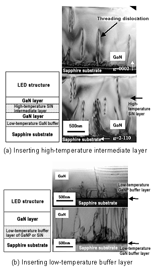 Picture b: The cross-section of undoped-GaN layer used low-temperature GaNP buffer layer and its TEM image.
Employing low-temperature buffer layer, the dislocation density is reduced by less than 1-5x109cm-2 to 5x108cm-2.
These methods of reducing the dislocation density enable bring much higher productivity without any complicated process.
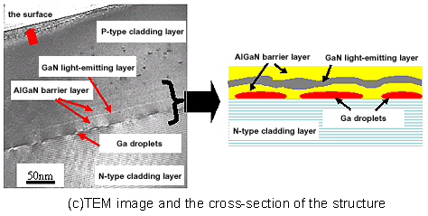
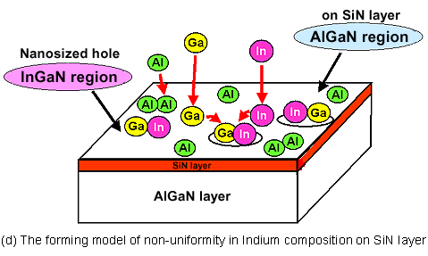
Increase the non-uniformity of In composition(Epitaxial Wafer)
In order to increase the non-uniformity of composition in the light-emitting layer, inserting nanosized region of Ga droplets and SiN discrete layer for varying the diffusion length of the composition help the fluctuation of band gaps and double the light-emitting efficiency of AlInGaN.
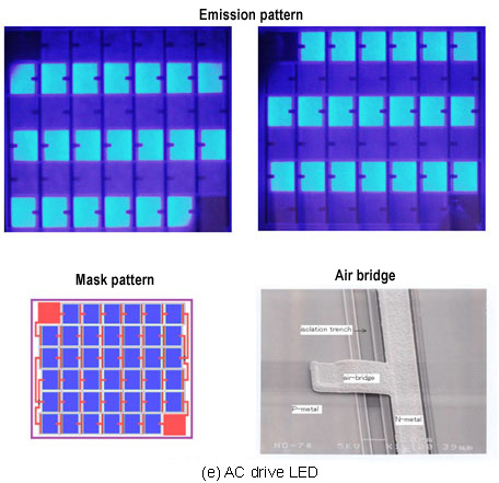
AC drive of LEDs (Current Circuit)
We license a LED manufacturer to use our technology of AC drive LED.
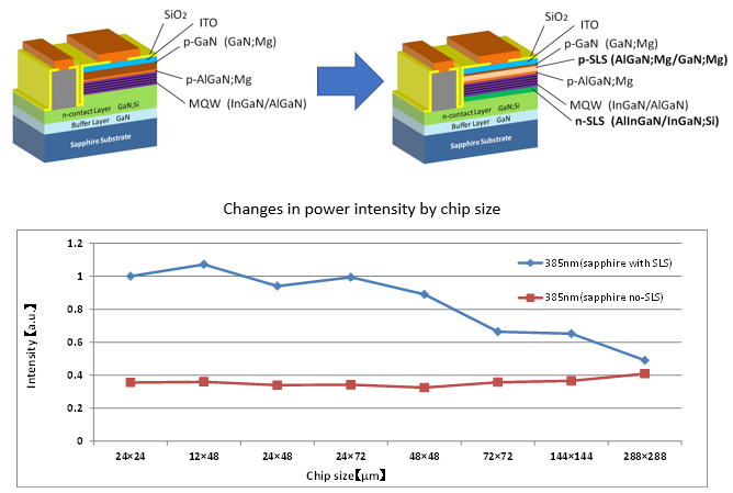
High efficiency of micro UV-LEDs (Epitaxial Structure)
In micro UV-LEDs, a technology that improves the optical output even if the chip size is micro by inserting pSLS layer and nSLS layer has been patented in Europe, the United States and Asia.
The band gap between n-layer and p-layer is widen by SLS. Therefore the carrier confinement effect seems to have increased.
![]()