
In general, gallium arsenide-based red LEDs and gallium P-based green LEDs have extremely low luminous efficiency when the chip size is 100µm square or less. In addition, there are problems such as difficulty in miniaturization due to the cleavage of the material and deterioration of characteristics due to UV rays during exposure. Various improvements and developments are being made to solve these problems.
On the other hand, blue and UV GaN-based LEDs have high luminous efficiency and are stable in terms of mechanical strength. However, in the display of "Blue LED + RG phosphor method", blue is LED light, green and red are photoluminescence, so the color variation of blue LED becomes a problem when it is used as a display.
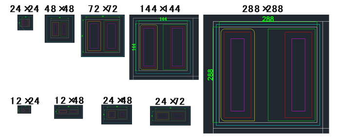
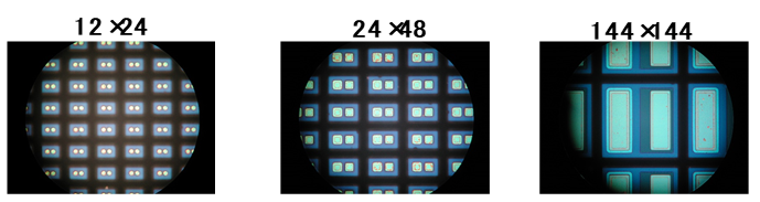
The images below are the drawings of 9 patterns of µUV LED chips manufactured on the same wafer using UV LED wafers with wavelengths of 385nm and 400nm. The chip size is 5 patterns of 24 x 24µm, 48 x 48µm, 72 x 72µm, 144 x 144µm, 288 x 288µm for squares, and 4 patterns of 12 x 24µm, 12 x 48µm, 24 x 48µm, 24 x 72µm for rectangles.
Features of µUV LEDs
 Chip size and pattern
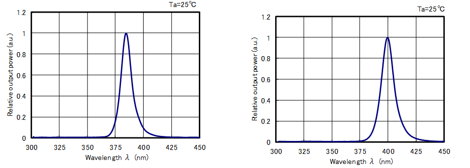
The graph below shows the emission spectrum of chips with wavelengths of 385nm and 400nm. For both the 385nm and 405nm chips, we can see that there is no difference in the spectrum even if the chip size is changed and have a good spectrum. 385nm chip has a peak wavelength of 384.72nm and a spectrum half width of 10.25nm, and 400nm chip has a peak wavelength of 400.07nm and a spectrum half width of 12.26nm.
Spectram of 385nm and 405nm chips
(left: 385 nm, right: 405 nm)
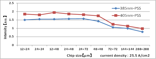
The graph beflow shows the result of measuring the emission intensity of each chip size with the current density fixed. It can be confirmed that the emission intensity is higher at 400nm than 385nm for all chip sizes, and the emission recombination rate due to the variation of indium composition is not affected even if the chip is microsized. More interestingly, there is a tendency for luminous efficiency to increase as the chip size decreases.
Measurement result of emission intensity for each chip size
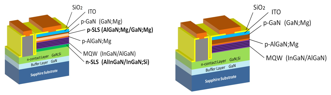
The image below shows the 385nm and 400nm µUV LED chip structures. Unlike the 400nm chip, the 385nm chip uses a superlattice structure (SLS) for the n-clad layer and the p-clad layer. With the µUV LED chip, it was confirmed that the luminous efficiency was increased by inserting the p-SLS layer and the n-SLS layer as compared with the case without SLS. It is considered that the band gap between the n layer and the p layer was widened by SLS, and the carrier confinement effect was enhanced.
Epitaxial structure of µUV LED chip
(left: 385nm, right: 400nm)
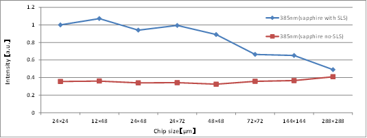
Emission intensity measurement result of 385nm µLED chip with and without SLS
![]()