
The images below are examples of µUV LED chip specifications for trial and mass production.
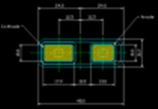
<Trial chip specification example>
•Chip size: 16µm x 48µm
•Distance between chips: length 10µm / width 30µm
•Chip area (chip size + distance between chips): 2,208µm2
•Effective area of 4-inch wafer: 6,936,260,000µm2
•Number of chips in 4-inch wafer: 3,141,422 pcs
µUV LED productivity
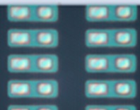
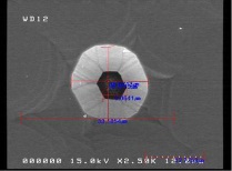
 Trial chip specification example (16µm x 48µm)
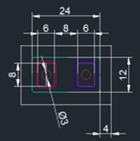
<Mass production chip specification example>
•Chip size: 12µm x 24µm
•Distance Between chips: length 5µm / width 5µm
•Chip area (chip size + distance between chips): 493µm2
•Effective area of 4-inch wafer: 6,936,260,000µm2
•Number of chips in 4-inch wafer: 14,069,492 pcs
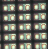
Mass production chip specification example (12µm x 24µm)
⇒The number of chips that can be taken is about 4.5 times that of
the trial.
⇒Manufacturing cost per chip is about 1 / 4.5
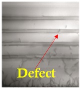
In order to improve the yield of chips, it is necessary to reduce the crystal defects and particles of the wafer. As shown in the image below, there are crystal defects called dislocations inside the epitaxial layer. If there are many dislocations, the electrical characteristics will deteriorate due to the increase in leakage current, and the luminous efficiency will decrease due to the decrease in emission recombination. Particles also cause poor appearance and poor electrical characteristics.
In order to improve the yield of chips, we are working on reducing dislocations by optimizing growth parameters and reducing particles by reviewing the work environment and work methods.
Types of defects (left: defects inside the epitaxial layer, right: epiwafer surface defects)
Transcription of µUV LED chips by LLO
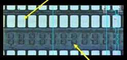
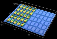
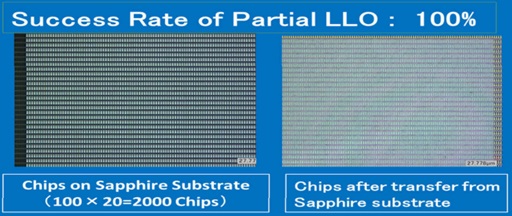
Image: Provided by V Technology Co., Ltd.
![]()